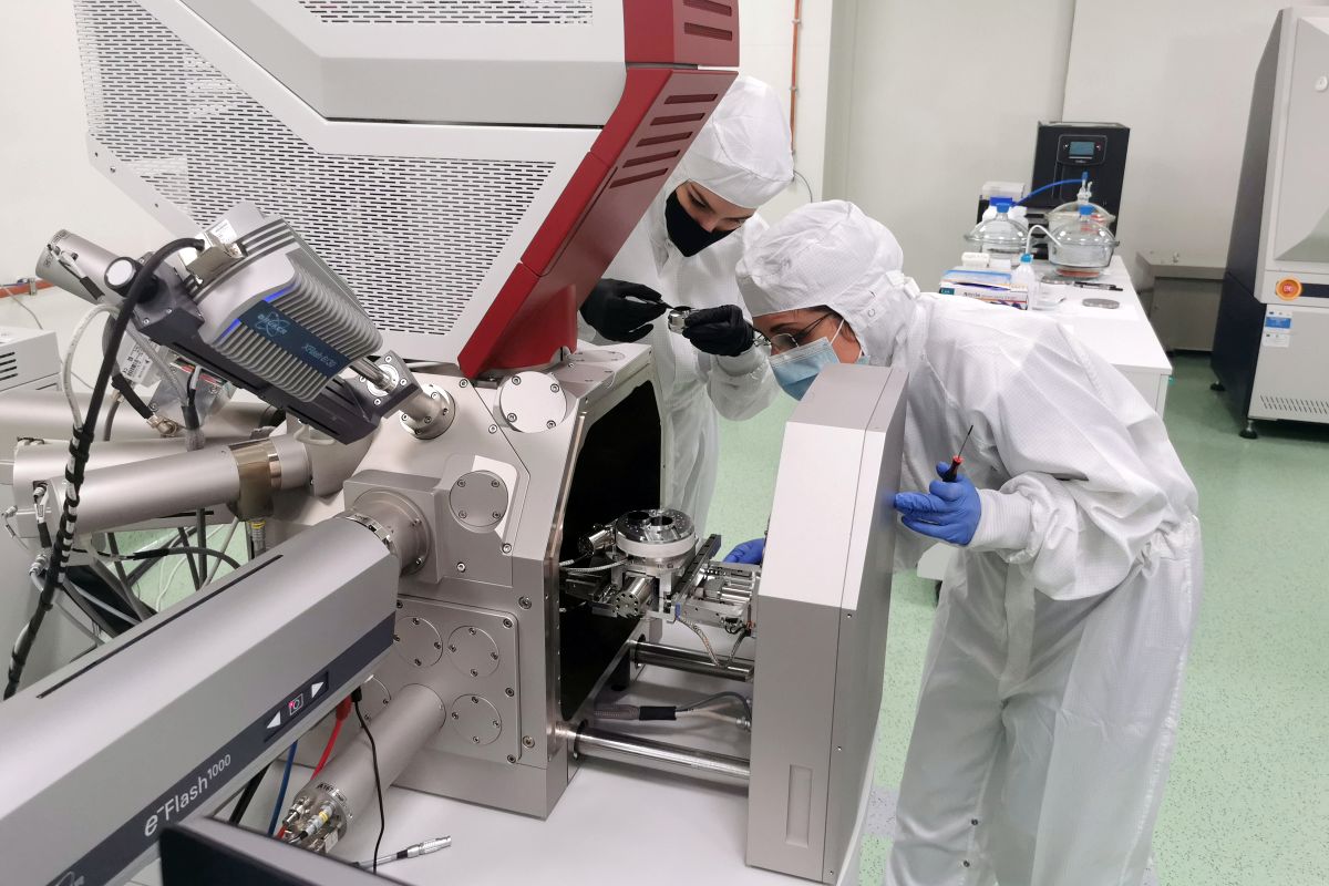
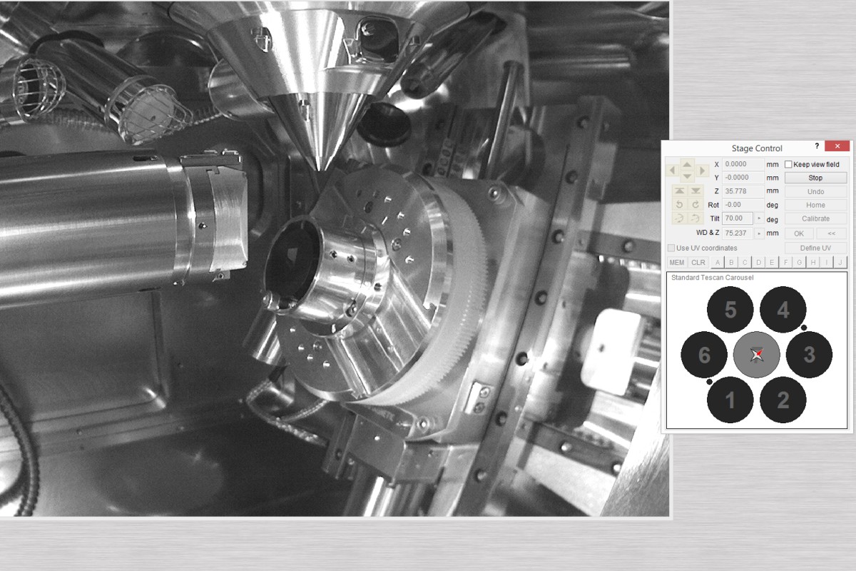
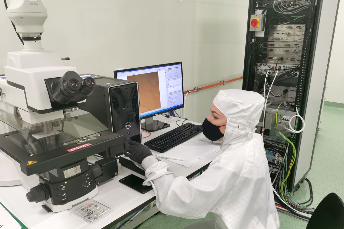
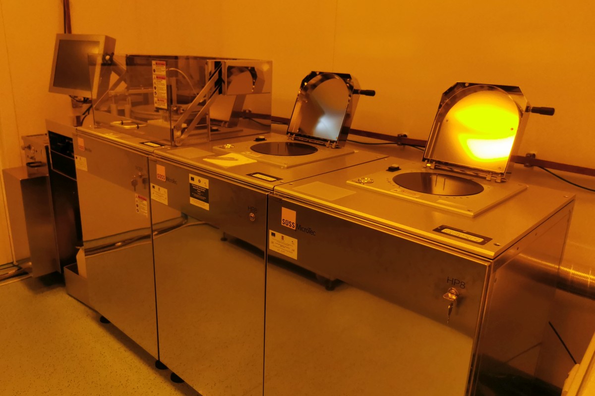
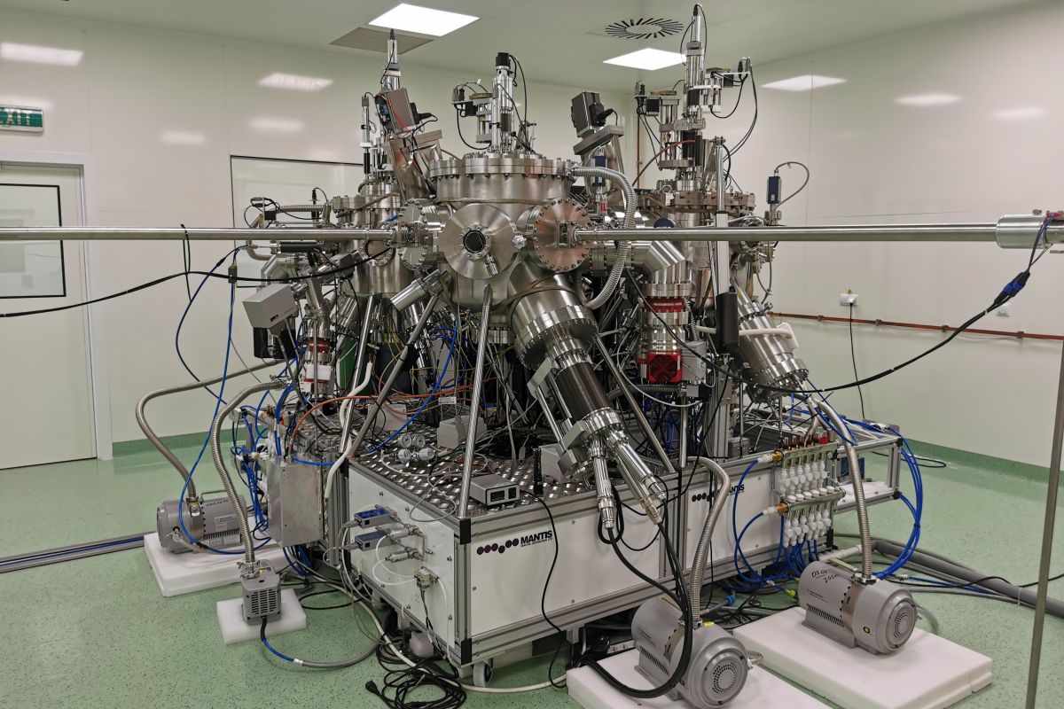
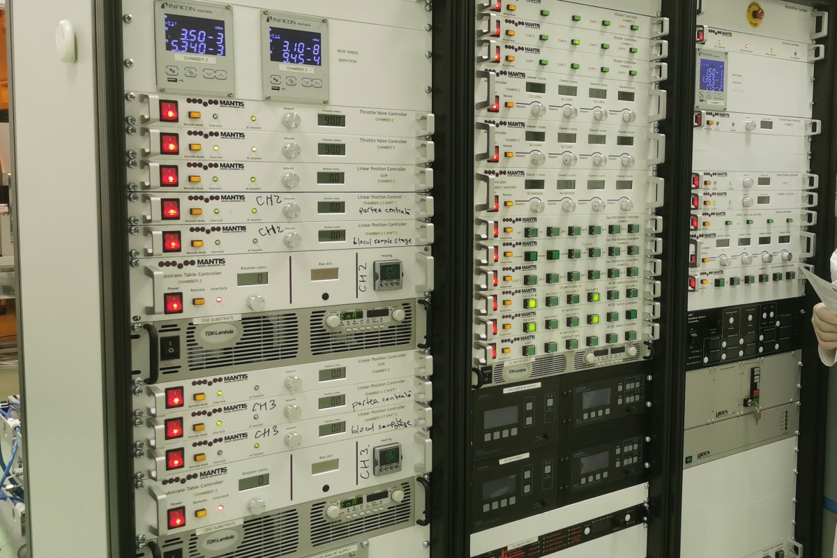
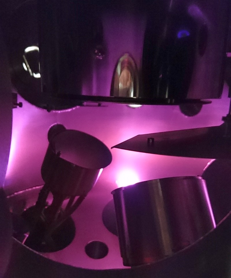
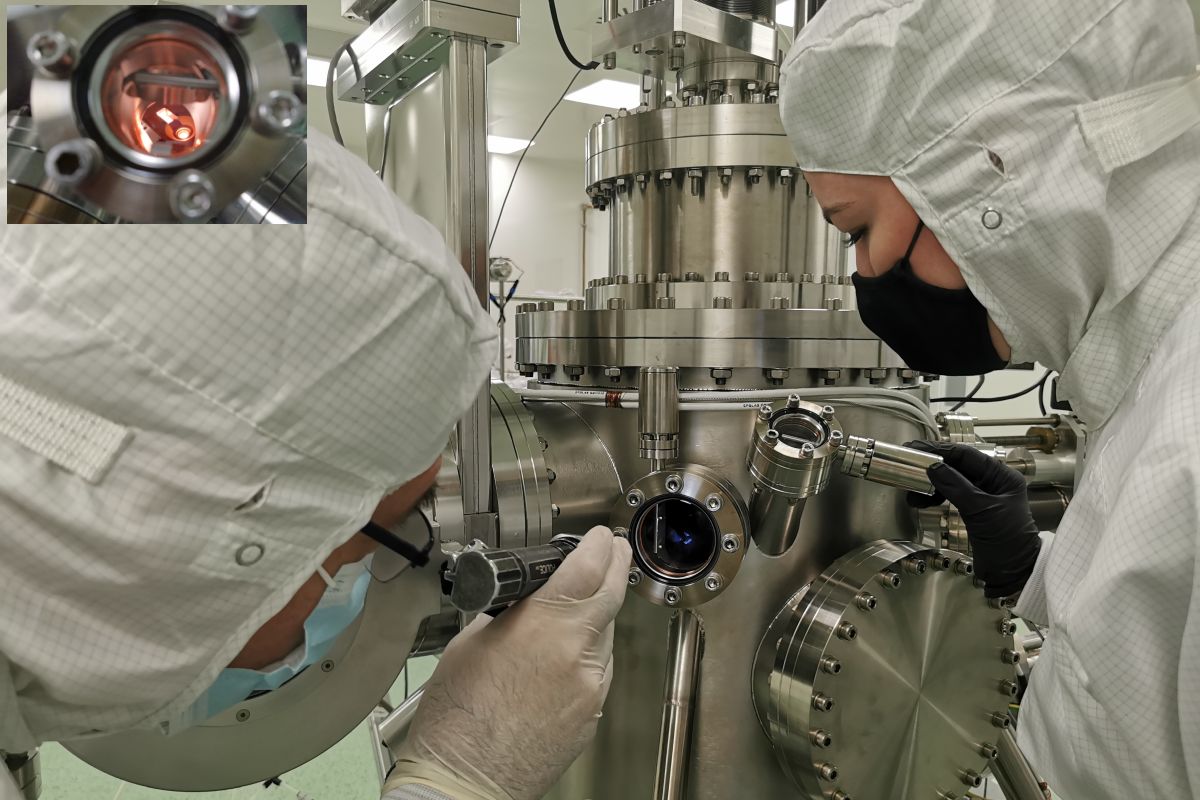
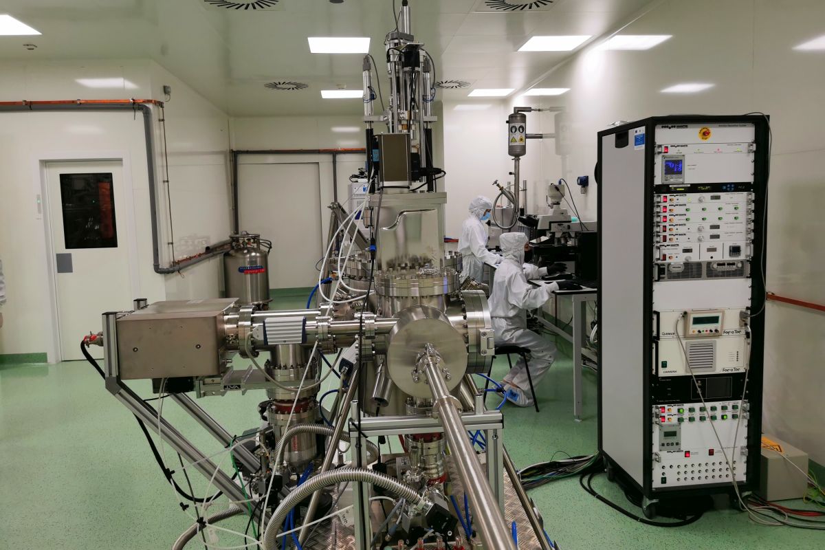
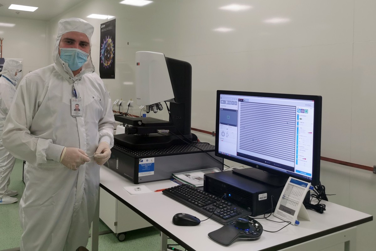
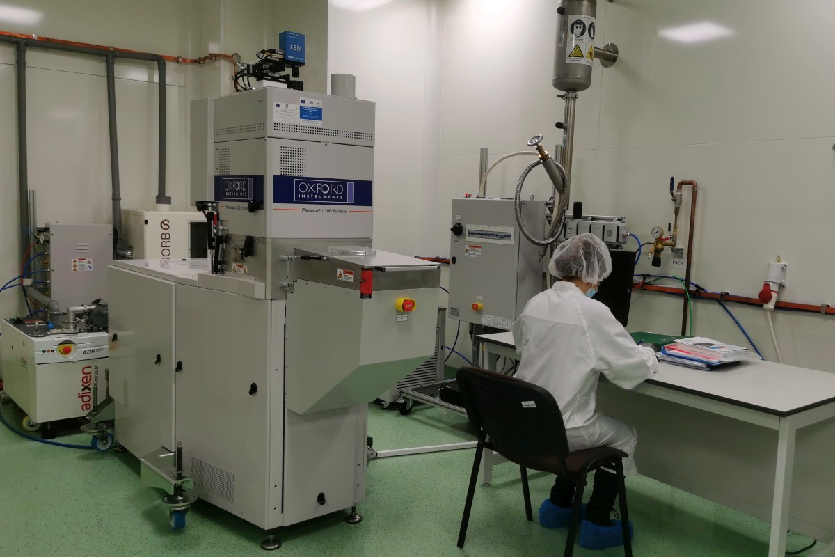
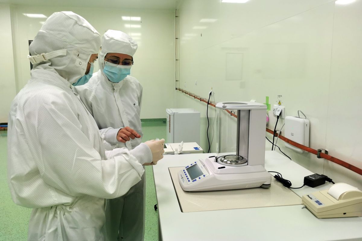
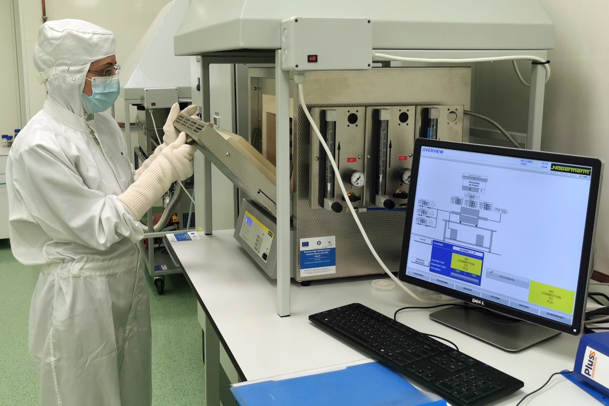
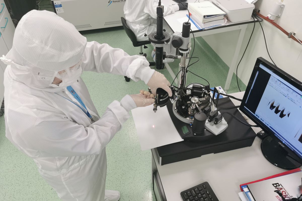
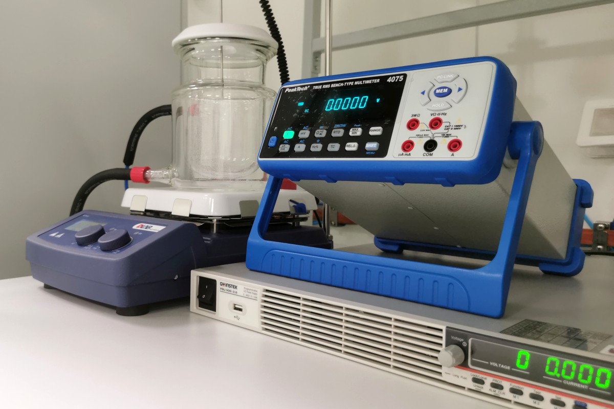
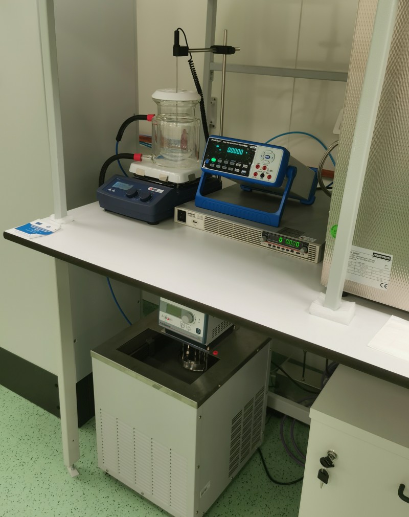
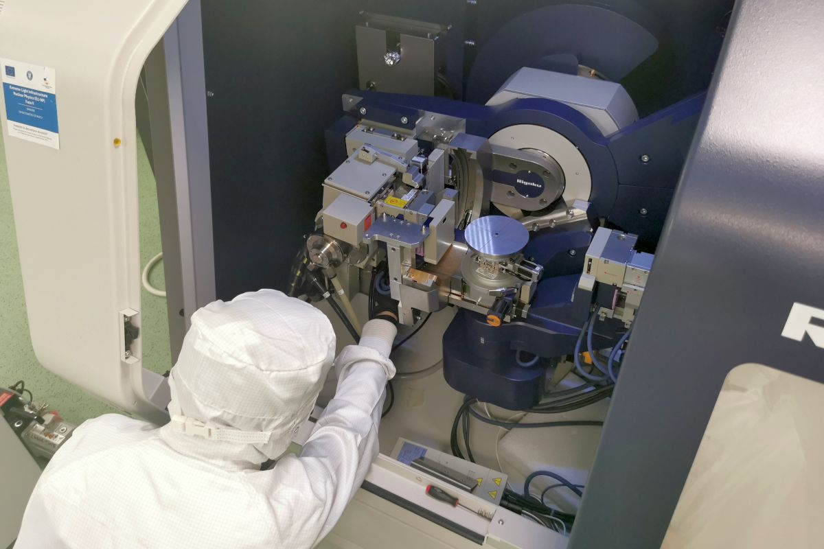
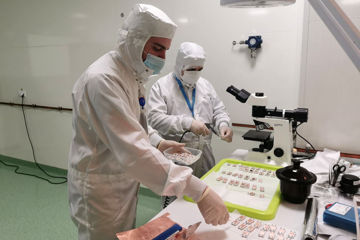
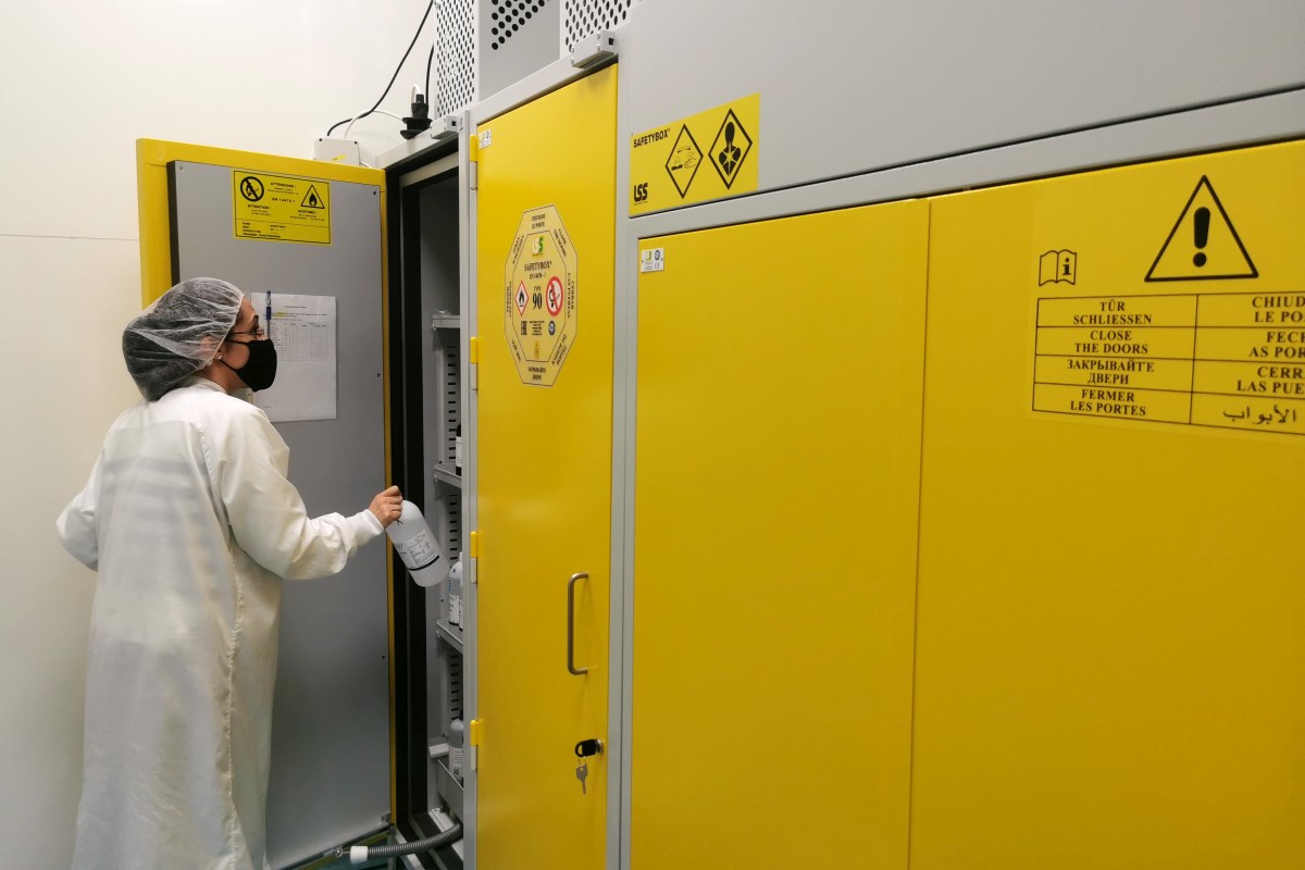
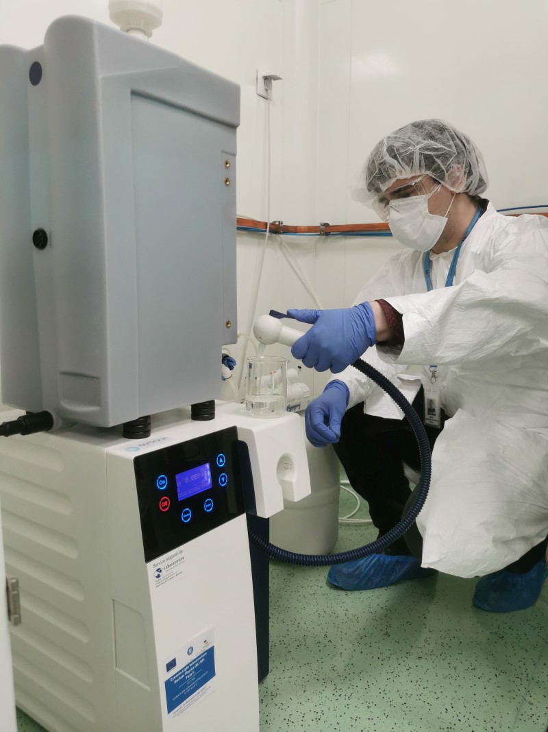
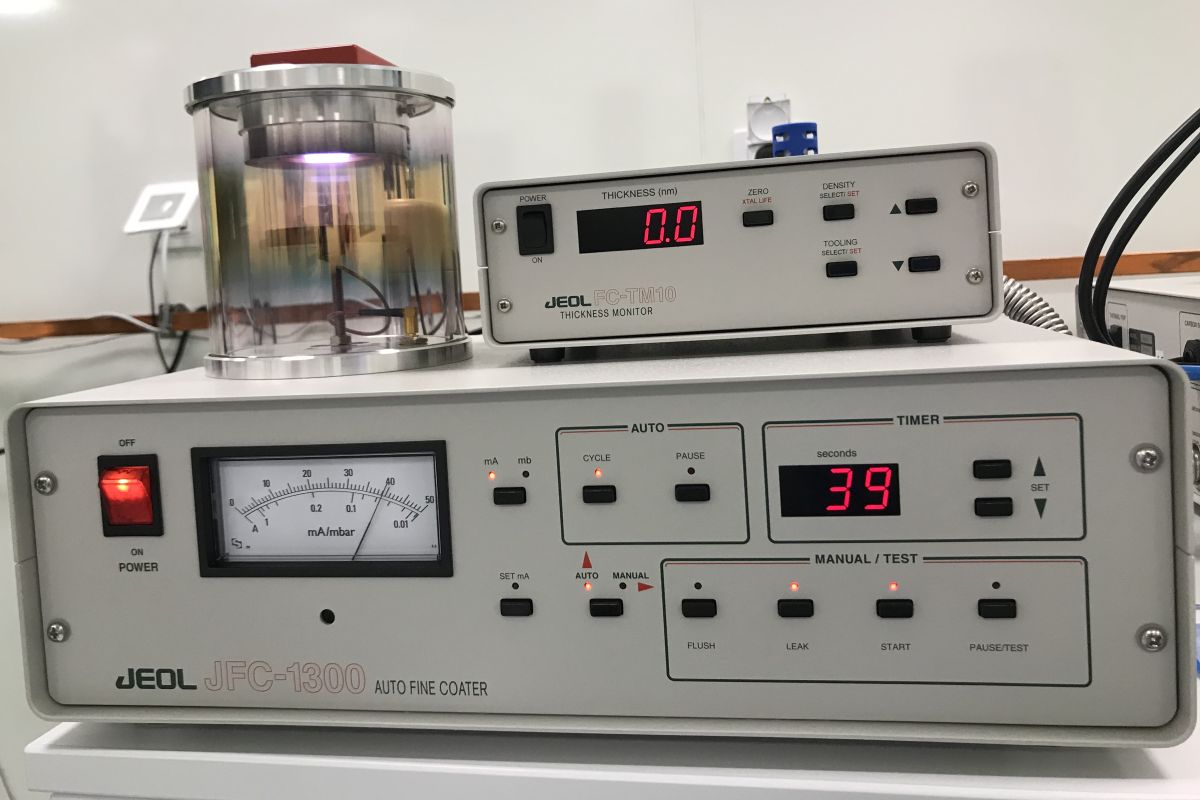
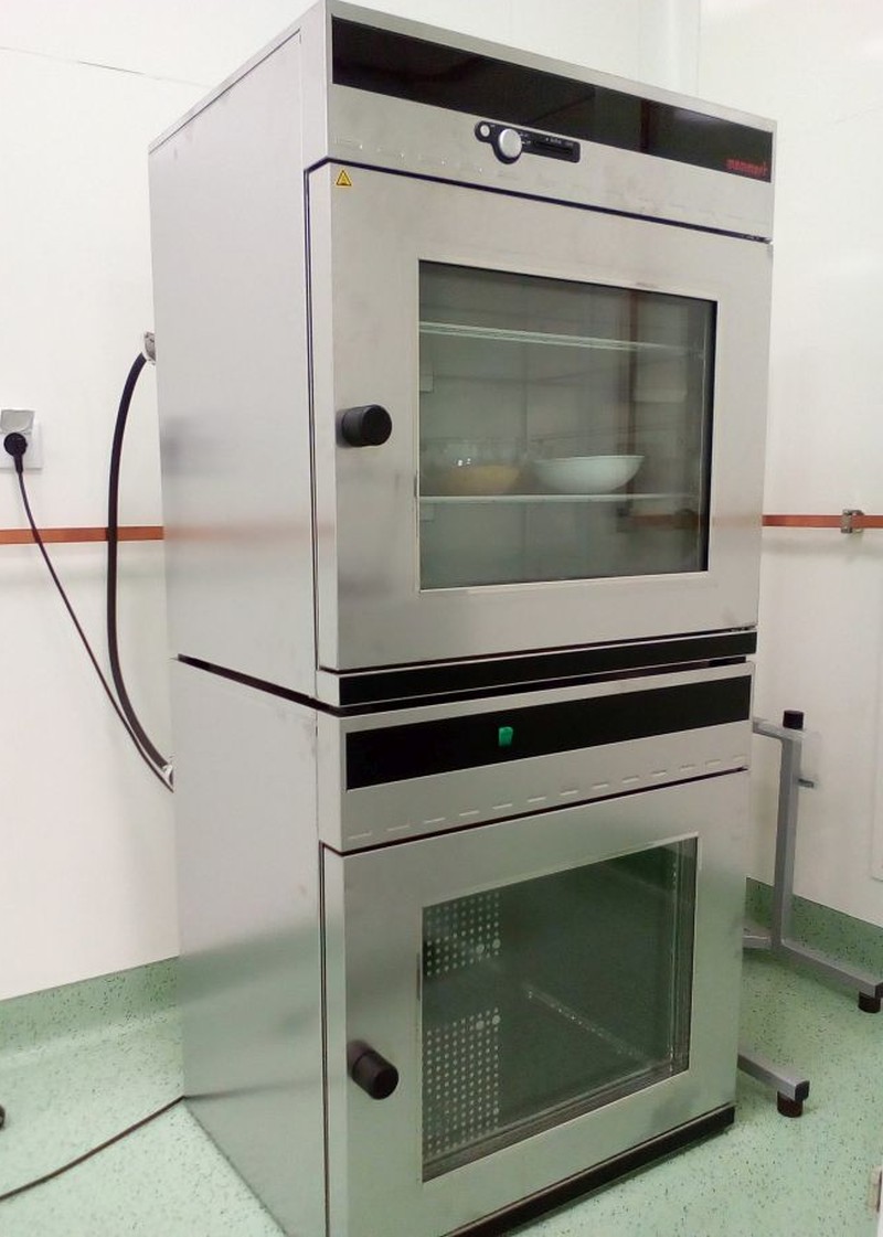
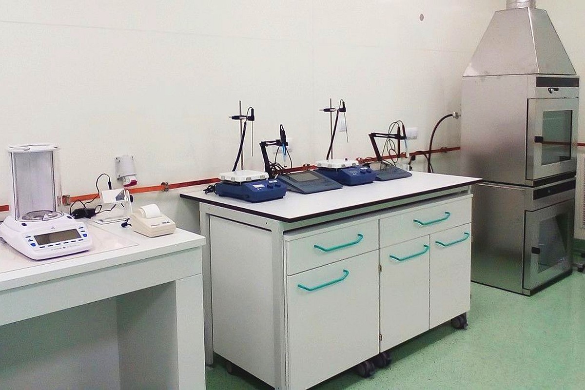
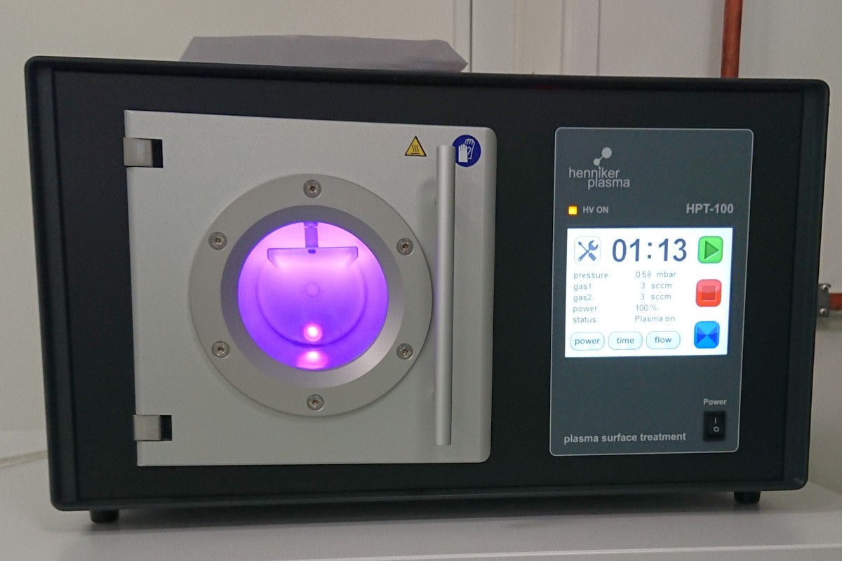
Embedded within the ELI-NP support complex, the Target Laboratory extends over 270 m2 of ISO 6 and ISO 7 cleanroom-environment.
This particular Lab is dedicated to the development, fabrication, characterization and micro-assembly of targets for experiments with
high-power lasers and gamma beams.
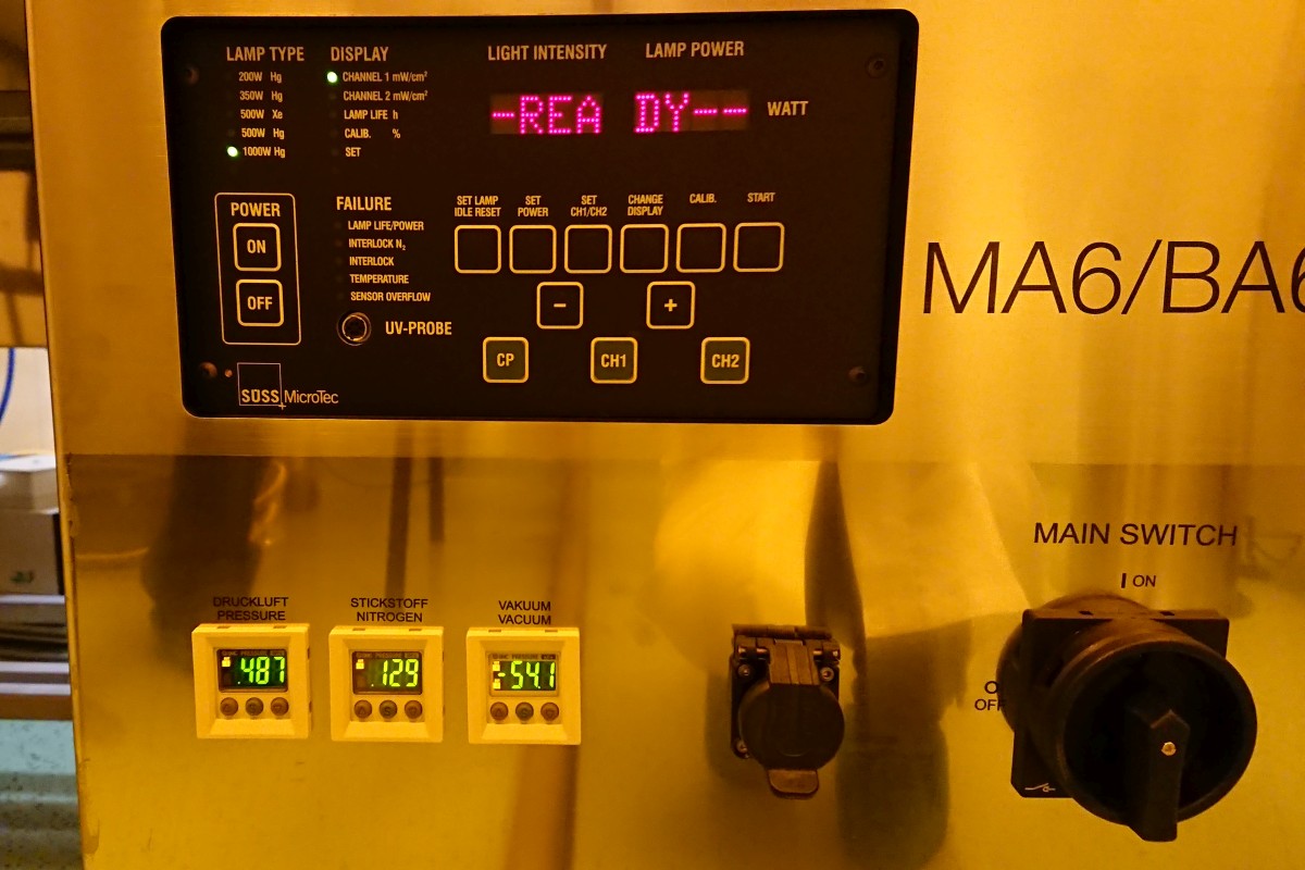
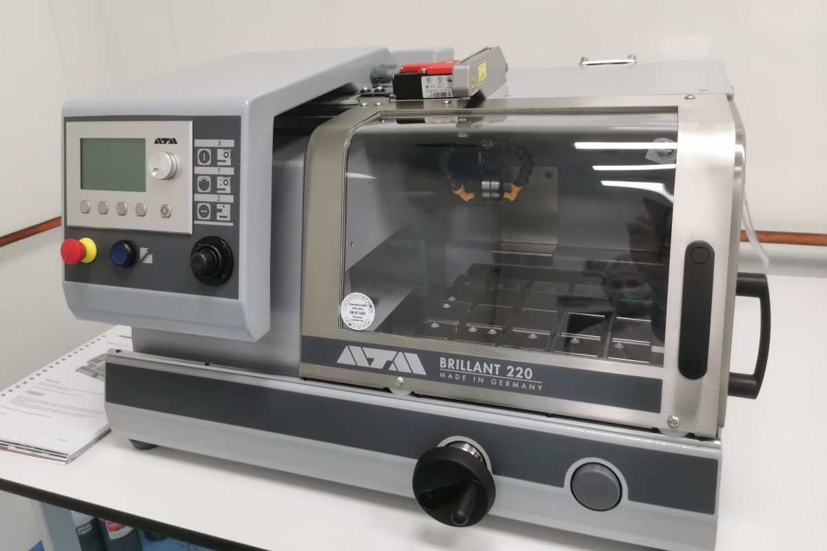
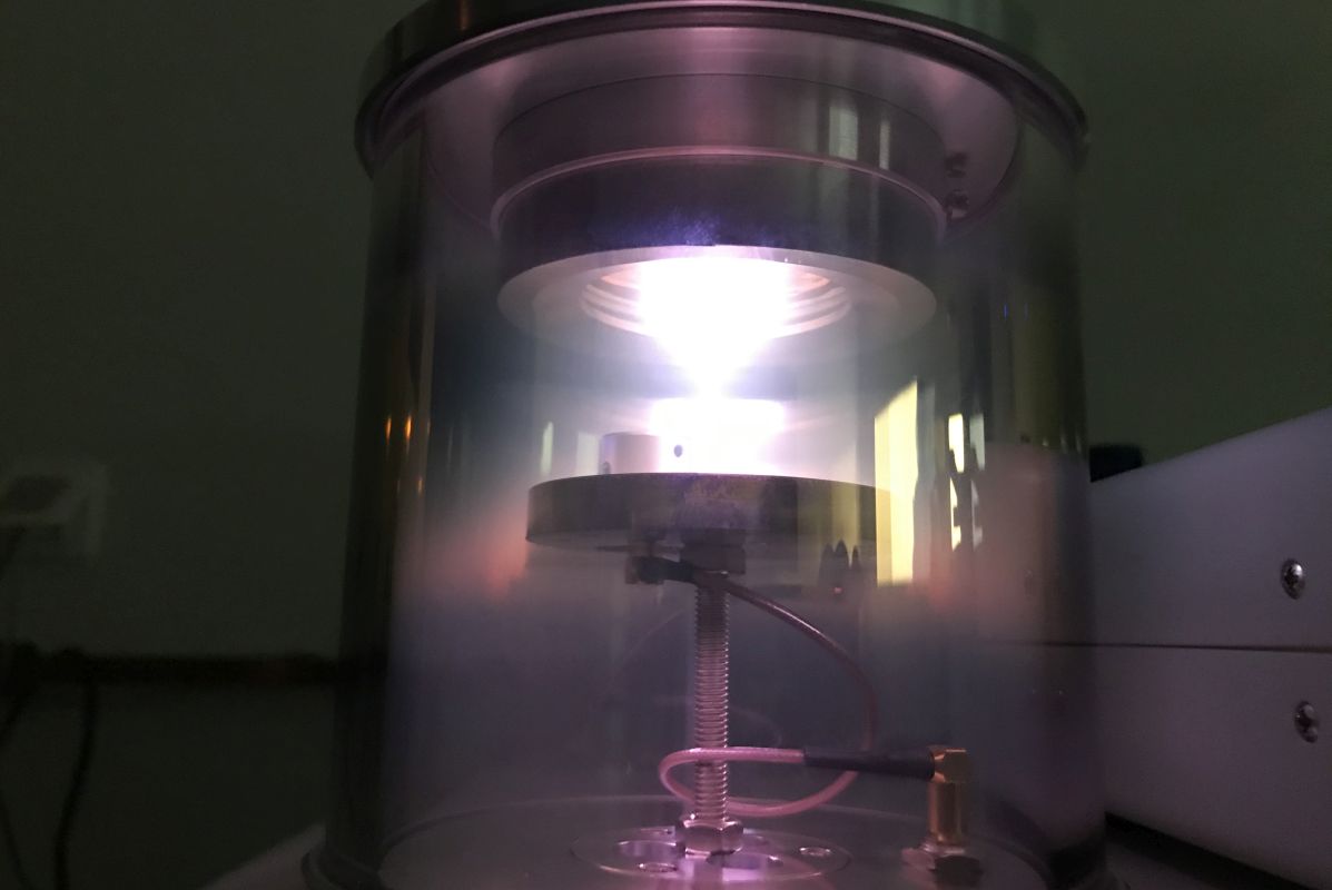
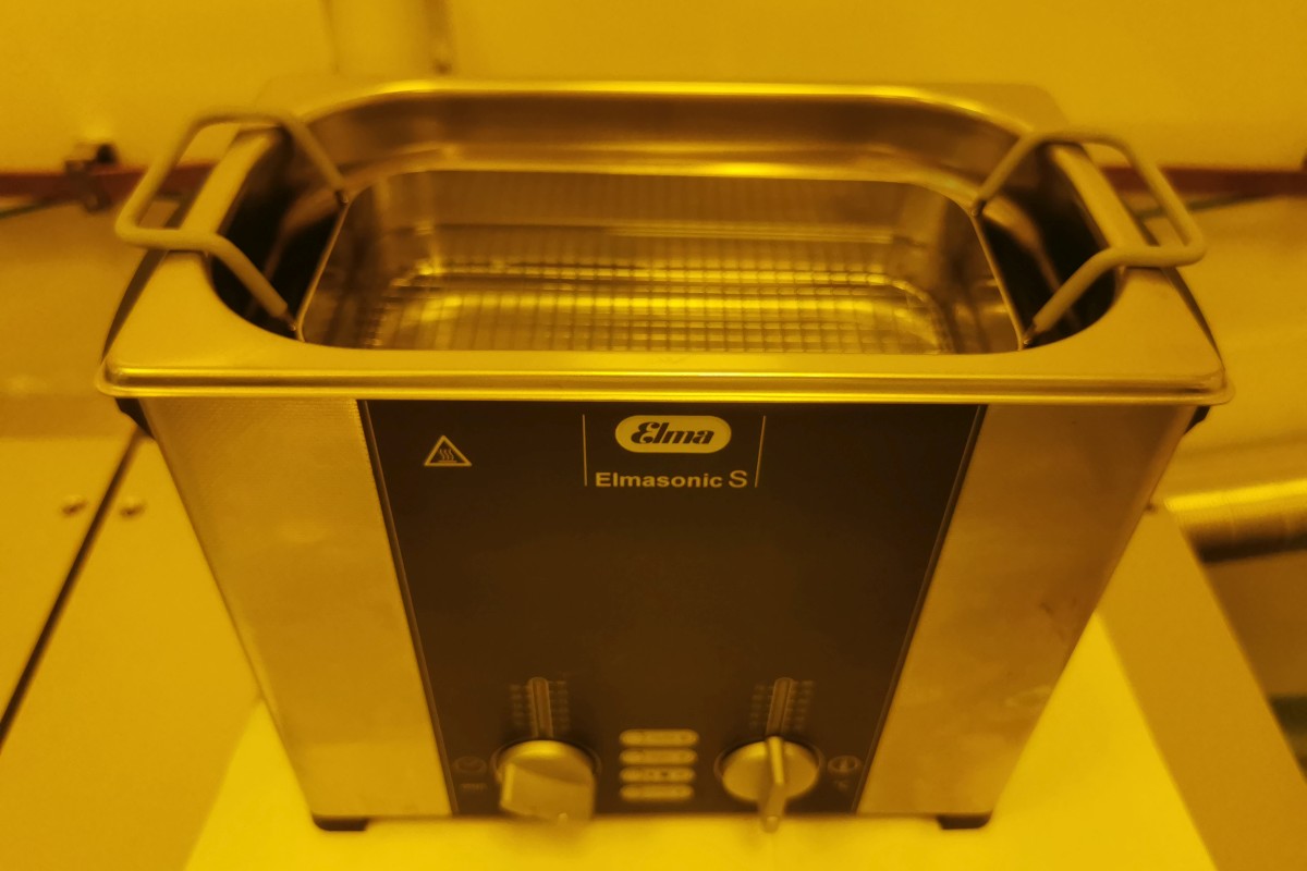
Accommodating a wide range of state-of-the-art equipment and a specialized team of materials scientists and engineers, the Target
Laboratory is set up to address demands for targets and provide support throughout the entire process,
from proposal evaluation, to technical feasibility and finally target delivery.
On top of that, it also performs Research and Development activities in order to continuously develop and upgrade novel target designs.


 eli-np.ro